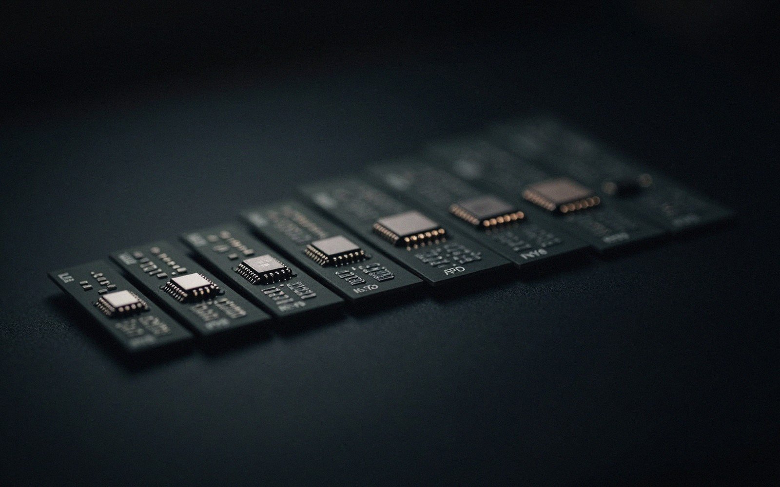
The silicon die is only part of the story. What surrounds it decides whether you can solder it, rework it, or even see what you're doing.[1]
| Package | Hand-solderable | Inspectable joints | Rework | Board area |
|---|---|---|---|---|
| DIP | Yes, with anything | Every joint visible | Trivial — or use a socket | Largest, and it needs through-holes |
| SOIC / TSSOP | Yes, with a fine tip | Every joint visible | Straightforward | Much smaller than DIP |
| QFN | With paste and heat, not an iron | Only from the edges, if at all | Needs hot air | Small, with a thermal pad underneath |
| BGA | No | Not without X-ray | Specialist equipment | Smallest per connection, more board layers |
§ 01From Through-Hole to No-Lead to Ball-Grid
A chip's package is the mechanical and electrical interface between microscopic silicon and the rest of your circuit board. Same die, different package: radically different experience at the bench.
 Enlarge ⤢
The DIP — dual in-line package — is the classic. Pins on two rows, 2.54 mm apart, drop straight into a breadboard or through-hole PCB. You can solder it with an iron and no magnification, pull it with a chip puller, swap it into a socket. Pin count tops out in the low forties before the package becomes impractically wide, which is why DIP mostly belongs to older designs and deliberately hobbyist-friendly parts.
SOIC and its shrunken cousins (SOP, SSOP, TSSOP) moved the same two-row layout to surface-mount pads on much tighter pitch. An SOIC at 1.27 mm pitch is still manageable with a fine iron tip and flux. Drop to 0.5 mm TSSOP and you're in drag-soldering territory: apply flux liberally, drag a small bead of solder across the row, wick away the bridges. Doable by hand, but it punishes impatience.
QFN — quad flat no-lead — puts pads on all four sides and, critically, underneath the package. The exposed pad on the bottom is often a thermal slug tied to ground; it dissipates heat well, but soldering it requires either a reflow oven or a hot-air station. You can't access the pad from the side. Inspection is awkward too — the solder joints hide under the package. X-ray is the gold standard for production; at the bench, you're mostly trusting your process and checking resistance to ground.
BGA — ball grid array — takes this further. Hundreds or thousands of solder balls arranged across the entire underside. All connections are hidden. Hand-soldering is essentially impossible; this is oven-and-stencil territory, often with X-ray inspection mandatory for confidence. BGA dominates where pin count, signal integrity and thermal density demand it: application processors, FPGAs, memory devices.
The tradeoffs run in two directions at once. Larger packages are beginner-friendly but physically large and electrically noisier at high frequencies — longer bond wires mean more parasitic inductance. Smaller packages shrink board area, reduce parasitics, and handle heat better through the exposed pad or ball array, but they demand better equipment, tighter paste control, and more rigorous inspection.
For prototyping, the practical advice is straightforward: choose the largest package your design tolerates. Keep BGA for when nothing else will carry the I/O count or the thermal load — and make sure your board house and your inspection setup can support it before you commit.
Notes
- Package choice is a soldering decision, a thermal decision and a rework decision — usually in that order. ↩