§ 01The wafer is where it starts
Silicon is the second most abundant element in Earth's crust, but the silicon in a microcontroller has almost nothing in common with beach sand. The journey begins at a facility that grows single-crystal silicon ingots using the Czochralski process: a seed crystal is lowered into molten, highly purified silicon and slowly pulled upward while rotating, drawing a cylindrical boule behind it. The result is a single unbroken crystal lattice, sometimes a metre or more long, with a purity measured in parts per billion of contaminant. That boule is then sawn into thin discs — wafers — and polished to a mirror finish. Most modern logic devices are built on wafers 200 mm or 300 mm in diameter; leading-edge fabs run 300 mm almost exclusively, because more wafer area means more chips per run and lower cost per die.
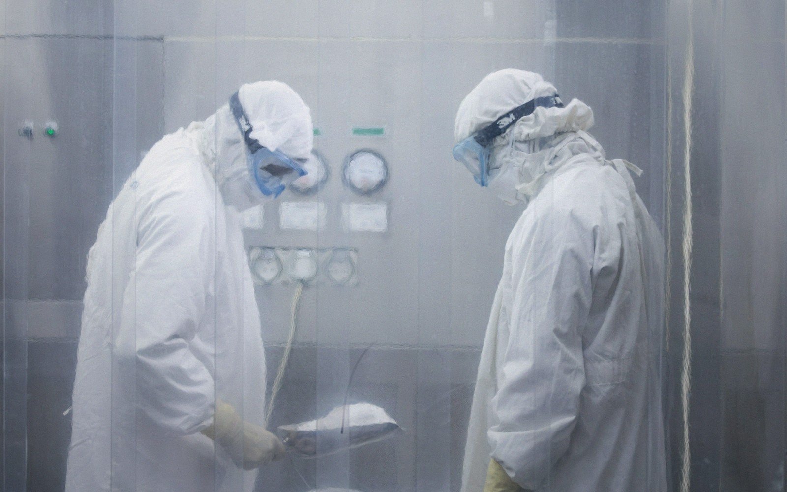
What happens next is not one process but hundreds, applied in sequence over weeks. The wafer enters a fab — a fabrication facility kept cleaner than a hospital operating theatre, classified by the size of particle a room will tolerate per cubic metre of air. Engineers and technicians wear full-body cleanroom suits not to protect themselves but to protect the wafer; a single human hair would dwarf the features being built on its surface.[1]
What happens next is not one process but hundreds, applied in sequence over weeks.
- Sand to ingotSilicon is purified and grown into a single crystal, then sliced into wafers and polished flat enough to print on.
- PhotolithographyA pattern is projected into photoresist and developed, over and over, one layer at a time.
- Doping and etchMaterial is added and removed where the pattern allows, building transistors in the surface of the wafer.
- Metal interconnectLayers of wiring are deposited to connect those transistors into circuits.
- Wafer probe testEach die is tested while still on the wafer; the ones that fail are marked before anyone spends money packaging them.
- Dicing and packagingThe wafer is cut into individual dice, and each good die is bonded into the package you will eventually solder.
- Final test and markingThe packaged part is tested again, graded, marked and put in a reel or a tube.
§ 02Printing circuits with light
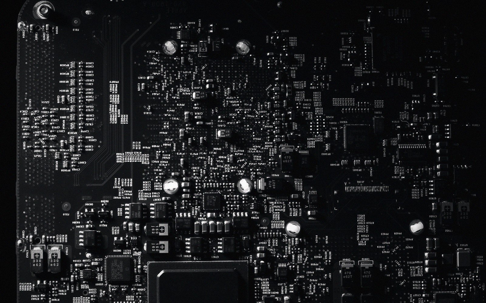
The core manufacturing step is photolithography, a process that uses light to transfer a pattern onto the wafer. First, the wafer is coated with a light-sensitive polymer called a photoresist. A mask — essentially a very precise stencil, sometimes called a reticle — carries the pattern for one layer of the circuit. An exposure tool, the stepper or scanner, shines ultraviolet light through the reticle and onto the resist. Where light strikes, the resist either hardens or softens depending on its chemistry. A chemical wash then removes the unprotected regions, leaving behind a precise polymer pattern that acts as a template for what follows.
 Enlarge ⤢
With the pattern in place, the exposed silicon (or the layer of metal or oxide beneath) is either etched away chemically or ion-implanted with dopants such as phosphorus or boron to change its electrical behaviour — creating the n-type and p-type regions that form transistors. The resist is then stripped away and the cycle repeats: deposit a new material, coat with fresh resist, expose through the next mask, etch or implant. A completed chip might demand thirty, fifty or more of these photolithographic layers, each precisely aligned to all the layers beneath. Alignment errors of a few nanometres can ruin a device, so scanners use laser interferometry to position each exposure with extraordinary accuracy.
The fineness of features that can be printed is determined by the wavelength of light used. Optical lithography using light at 193 nm wavelength — pushed through water-immersion systems and combined with multi-patterning tricks — can produce features at dimensions that seem impossible for the wavelength involved. At the leading edge of production, EUV (extreme ultraviolet) lithography uses 13.5 nm wavelength light generated by firing high-power lasers at tin droplets; the machines that do this, built by ASML in the Netherlands, are among the most complex manufacturing tools ever made. The transistors on the most advanced chips today are measured in single-digit nanometres — a feature several hundred times thinner than a red blood cell.
The interconnect layers come last in the front-end sequence. Transistors sitting in the silicon are useless without wiring, so the fab deposits alternating layers of dielectric insulator and metal — historically aluminium, now mostly copper for its lower resistance — etched into the routing patterns that carry signals between transistors. A high-performance chip may have a dozen or more metal layers stacked up, the lower ones carrying fine local connections and the upper ones carrying the wider power and clock buses that span the whole die.
§ 03Testing before the saw
When all the layers are complete, the wafer still looks like a mirror with faint coloured patches — the individual chips, called dies, are not yet separated. Before they are, every die on the wafer is tested electrically by a wafer prober: a machine that lands fine needles or a probe card on the bond pads of each die in turn and runs a suite of parametric and functional tests. Dies that fail are marked with ink or, more commonly, logged in a digital wafer map. This step, called wafer sort or die sort, identifies known-good die before the expense of packaging is applied to parts that will never work.
The wafer is then diced — sawn along the grid lines between dies using a diamond-tipped blade or a laser. Individual good dies are picked up, the bad ones discarded. Yield — the percentage of working dies on a wafer — is one of the most closely guarded metrics in the industry. A new process typically starts with low yield; engineers hunt the systematic defects that cause failures, fix them, and push yield up over months and years. Yield is where profit lives.
§ 04The package makes it handleable
A bare silicon die is mechanically fragile, its bond pads far too small and too closely spaced to solder onto a printed circuit board. The package solves both problems. In wire bonding — still the dominant method for most microcontrollers and analogue parts — the die is glued to a lead frame, and fine gold, copper or aluminium wires are ball-bonded under heat and ultrasonic energy from each die pad to a corresponding lead. The assembly is then encapsulated in moulded epoxy, which protects the die from moisture, handling and electrostatic discharge. What emerges is the familiar black plastic rectangle with metal pins or pads arranged around it.
Flip-chip packaging, used on higher-density or higher-performance devices, takes the opposite approach: the die is flipped face-down onto the substrate, and microscopic solder bumps on the die surface connect directly to matching pads below. This shortens the electrical path, allows many more connections in a smaller area, and spreads heat more effectively — but the equipment and substrate costs are considerably higher. Ball-grid array (BGA) packages take this further, spreading connections across the entire underside of the package rather than just the perimeter. The packages a device comes in have real consequences for how you solder and rework it at the bench.
§ 05Final test and the long chain behind every part
After packaging, the chips go through final test: a full electrical and parametric workout at temperature, often at both cold and hot extremes, to catch any marginal devices. Some parts are tested at speed-grade limits to select which frequency bin they fall into — this is why you sometimes see the same die sold under different part numbers at different clock speeds. Parts destined for automotive or military use may face extended burn-in, where devices are powered up under heat for many hours to force early-life failures to appear before the part reaches a customer.
What lands in your supplier's tape-and-reel has been through, conservatively, four to six weeks of fab time, days of test, and a global supply chain that typically spans multiple countries for crystal growth, fabrication, packaging, test and distribution. A given chip may be designed by a fabless company — one that owns no fab, only the intellectual property — manufactured at a foundry such as TSMC in Taiwan or GlobalFoundries in the US and Germany, packaged in Malaysia or South Korea, and tested in several of those places along the way. Arm, headquartered in Cambridge, designs the processor cores that sit at the heart of many of these chips without manufacturing a single one. The physical device you pick out of a reel is the downstream product of an extraordinarily distributed industrial process, one that has no real equivalent anywhere else in manufacturing.
Understanding even the outline of that process changes how you read a datasheet. Operating voltage ranges, temperature grades, ESD limits, storage conditions — all of them trace back to specific decisions made in the fab, the package house and the test floor.
An independent explainer on chips, programming and embedded systems. Not a manufacturer, distributor or reseller.
Notes
- This is the shape of the process, not a recipe. The details belong to the fabs and change constantly. ↩